2026: Optimizing Semiconductor Manufacturing Processes to Eliminate Emissions of PFASs and High Global Warming Potential Gases
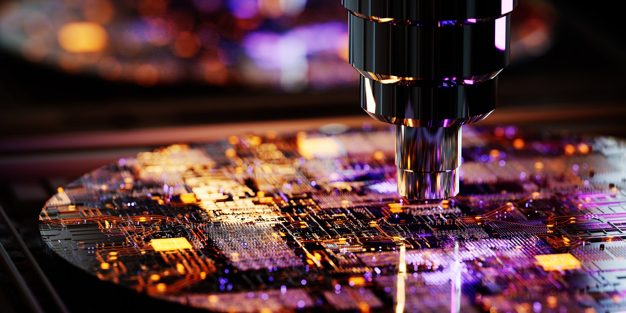
Semiconductor manufacturing relies on plasma etching processes that use fluorinated gases with high global warming potential and may unintentionally generate per- and polyfluoroalkyl substances (PFAS), which are environmentally persistent and difficult to manage. This project seeks to redesign plasma etching methods to eliminate or greatly reduce emissions while maintaining the performance and reliability required for advanced chip manufacturing. Researchers from the School of Civil and Environmental Engineering and Cornell NanoScale Facility will investigate how PFAS form during etching, identify process conditions that drive their creation, and test lower-global-warming alternatives to conventional etch gases. The team will then evaluate whether these alternative processes also reduce PFAS emissions without compromising nanoscale device fabrication. An advisory board of chip manufacturers and gas suppliers will help ensure the solutions are scalable and commercially viable. The project aims to provide the semiconductor industry with practical tools to reduce both greenhouse gas emissions and persistent chemical pollution.
Investigators: Damian E. Helbling (Cornell Duffield Engineering/Civil and Environmental Engineering), and Judy Cha (Cornell Duffield Engineering/Materials Science and Engineering)